The merger of Stanford Nano Shared Facilities (SNSF) and the Stanford Nanofabrication Facility (SNF) last September created nano@stanford, the university’s largest shared research facility on campus.
Yuri Suzuki, the Stanley G. Wojcicki Professor in the School of Humanities and Sciences and professor of applied physics and, by courtesy, of materials science and engineering, serves as the inaugural director of nano@stanford. Suzuki also directs the Center for Energy Efficient Magnonics at SLAC National Accelerator Laboratory.
“The merger enables us to better support principal investigators by accelerating research,” Suzuki said. “That’s what’s important. That’s what we’re here for.”
Here, Suzuki discusses the open-access facility and how it supports cutting-edge, multidisciplinary research and education in nanoscale science and engineering.

Yuri Suzuki is the director of nano@stanford. | Courtesy nano@stanford
Why merge the two facilities now?
SNF has its origins in the School of Engineering, going back to the 1980s as a professional-grade cleanroom for fabricating electronics devices. It is a facility that enables researchers to make things they will use. SNSF arose from the effort to aggregate several characterization laboratories under one umbrella. SNSF enables researchers to analyze their work. Making and analyzing are not only complementary but necessary for quality experimental work.
Since their inception, SNF and SNSF have evolved to meet the needs of our researchers, each acquiring capabilities that span their traditional domains of both “making” and “analyzing.” The merger on September 1, 2025, follows the natural progression of the needs of our research community for easy access to the spectrum of fabrication and characterization capabilities.
SNF was most recently part of the School of Engineering, while SNSF was governed by the Vice Provost and Dean of Research. In the past, there’s been discussion about merging them, but it had never materialized. Philip Wong, a professor in the School of Engineering, was the director of SNF while I was the director of SNSF. Together, we thought a single research infrastructure unit would better serve the community by accelerating their research and eliminating overlapping tools and infrastructure. This time, the stars aligned. Both Dean of Engineering Jennifer Widom and Vice Provost and Dean of Research David Studdert agreed.
What does the merger mean for researchers?
Over the years, the two facilities had evolved their own administrative and laboratory ecosystems. This was challenging for researchers using both facilities, who had to use different protocols to perform the same operation.
Now, researchers in nano@stanford have a unified user experience, with minimal administrative barriers and a more uniform cost structure and policies. Most importantly, we can better support our researchers by engaging at a holistic project level rather than a one-instrument-at-a-time approach. Finally, the merged organization helps make Stanford more competitive with our peers in pursuing grants and other opportunities.
We provide access to state-of-the-art lithography, etching, and thin-film deposition tools, as well as state-of-the-art characterization tools, in a single facility at nano@stanford. Not only do we help our users identify the appropriate fabrication tools but also suitable characterization tools for their sample. The shared facility is a partnership between faculty, users, and staff, and it is designed to help all of us stay on top of innovation. nano@stanford facilities are located across five locations on campus: Allen, Shriram, Spilker, McCullough, and Deep Lab. The administrative headquarters will be in Deep Lab when it officially opens in March.
How would you explain nanotechnology to someone unfamiliar with the field?
Nanotechnology is a very broad term. People often think of semiconductor electronics – chips in your computer – but it really means anything at the nanometer-length scale, which is about 10,000 times thinner than the width of a human hair. At these length scales, forces like static electricity and surface tension, which are barely noticeable in everyday life, become dominant. Understanding and controlling these nanoscale effects allows us to create advanced electronics, uncover new scientific insights, and drive innovation.
Miniaturization requires tools to pattern materials at the nanometer-length scale. The materials may be films or clusters of molecules. Whatever the medium, we need to develop reproducible fabrication processes. We also need to know what we’ve made using our characterization tools.
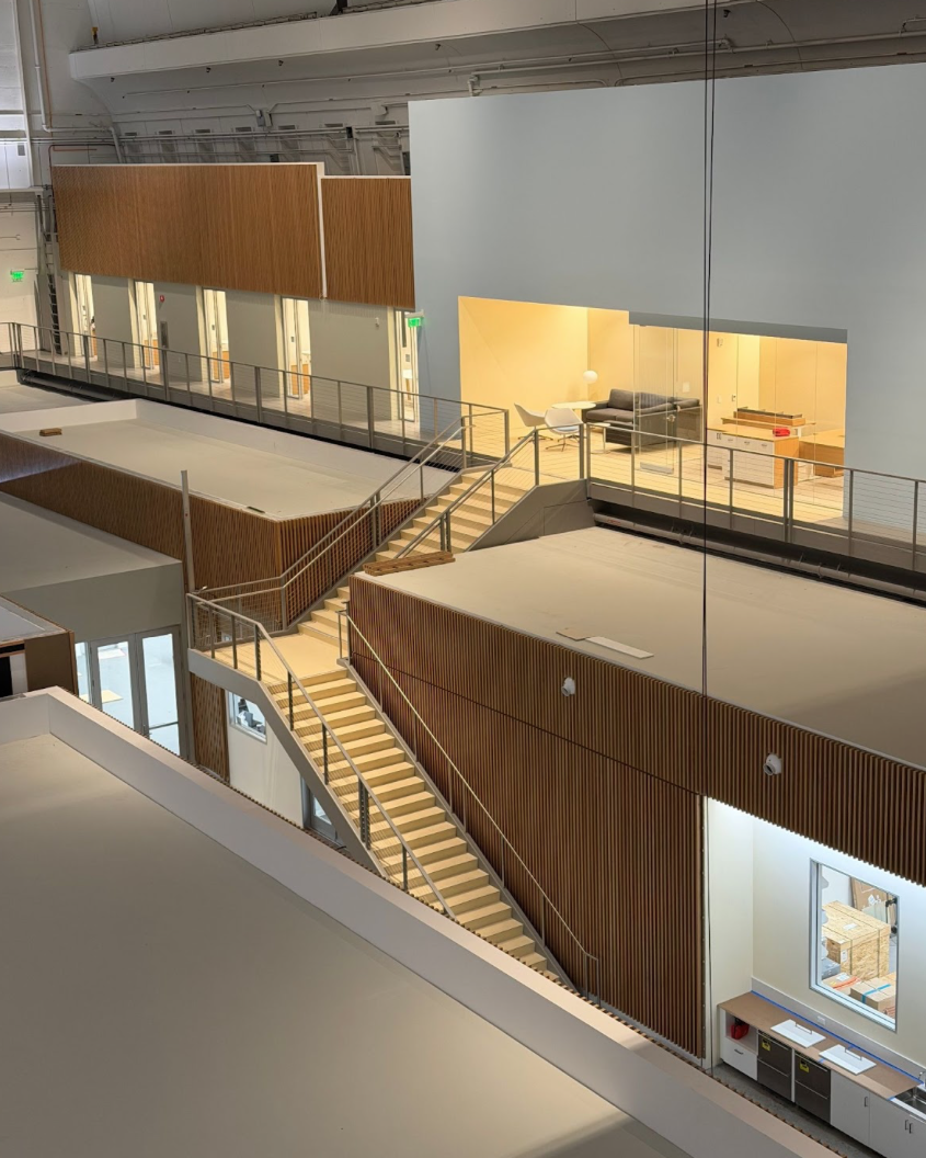
Administrative headquarters of nano@stanford will be in Deep Lab when it officially opens in March. | Courtesy nano@stanford
At nano@stanford, there are both fabrication and characterization tools. Nanofabrication involves the processing of materials with nanoscale features. Then these nanofabricated materials are characterized to confirm what you made is what you think you made. It’s not just knowing how small you made them, but understanding their behavior at very small length scales.
Stanford has a rich history in nanotechnology research. What are some notable breakthroughs?
One of the significant inventions at Stanford is the atomic force microscope, or AFM. It was invented by one of my Applied Physics colleagues, Calvin Quate, with Gerd Binnig and Christoph Gerber, and came into manufacturing when I was a grad student in the early 1990s. We are currently putting together an exhibit about its development for the newly expanded facilities at the Deep Lab. nano@stanford recently honored Quate’s memory at a symposium celebrating 40 years of atomic force microscopy.
The microscope allows you to image samples at the atomic scale by probing forces between a cantilever and the underlying sample; hence, Quate, Binnig, and Gerber developed a sensitive cantilever that enables you to do this. Beyond imaging topography, the AFM can also provide advanced imaging of magnetic and electrical forces, conductivity, capacitance, and much more. For example, a magnetically coated cantilever can be used to detect magnetic structure on the surface of a sample – something that is very useful in my research. I still remember the first AFM I used at Stanford, which was suspended on a tripod using bungee cords.
The AFM is one of nanotechnology’s most important breakthroughs – and the first AFM probes were developed and tested at Stanford using the fabrication and characterization facilities. With this merger, we aim to provide seamless access to both fabrication and measurement tools, enabling future innovations as transformative as the AFM.
How can the Stanford community learn more about nano@stanford?
We post announcements and other information to the nano@stanford website. We hold town halls and send periodic announcements to the community through various listservs. The website is the best place to learn more, and my door is always open.
Writer
Deborah Petersen