Ten people get into bunny suits, many for the first time in their lives. Under the hoods, their hair is in hair nets. Goggles cover their eyes, their gloves are tucked into their sleeves. For those with facial hair, that’s netted too.
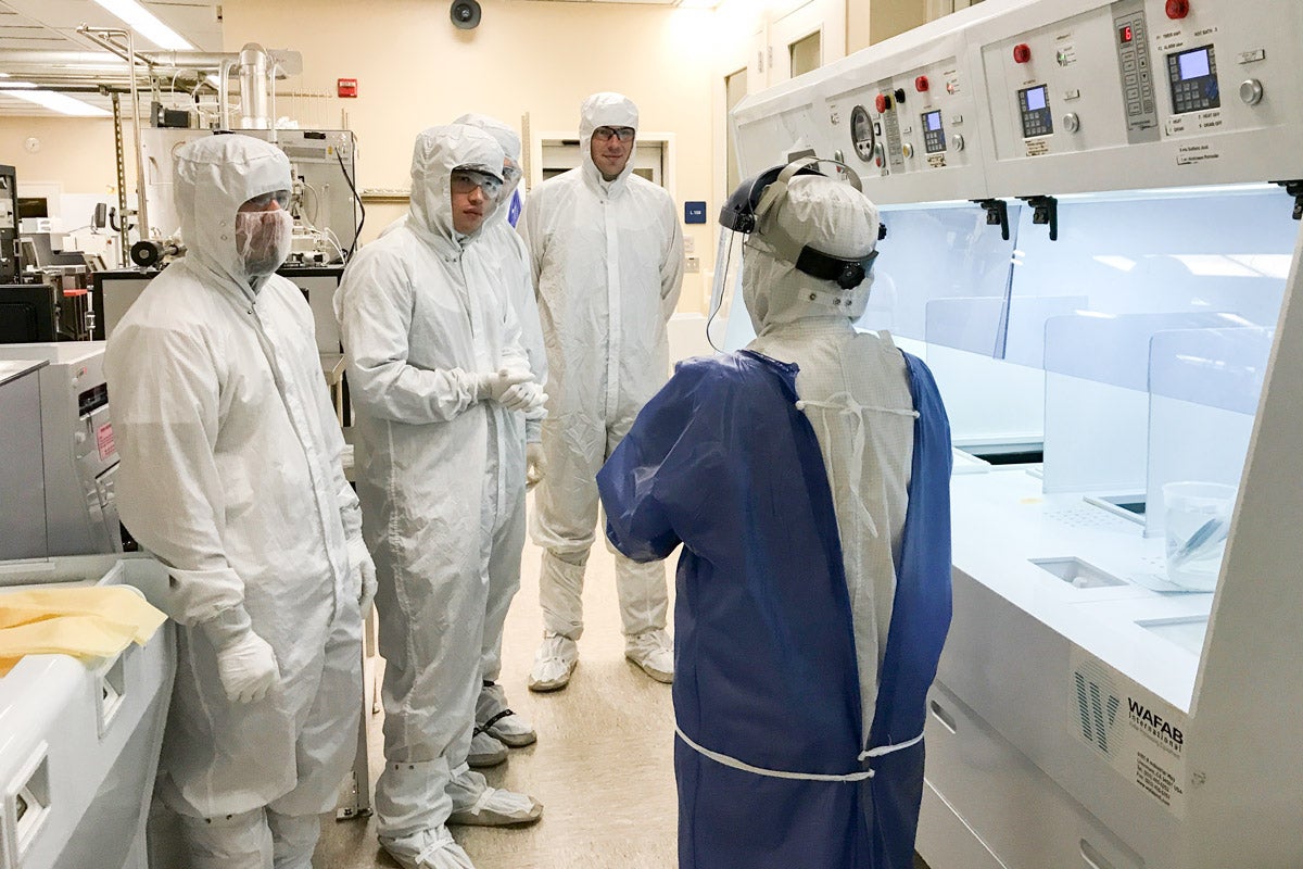
Students from California State University, East Bay, watch Uli Thumser prepare silicon photovoltaic cells during a tour of the Stanford Nanofabrication Facility. (Image credit: Angela Hwang)
With all hair, lint and dust safely tucked out of the way, the students are ready to enter the Stanford Nanofabrication Facility. This particular group was part of a class from California State University, East Bay, co-taught by Ryan Smith, assistant professor of physics at CSU-EB, and Erik Helgren, associate professor and chair of physics at CSU-EB. The class visited as part of a collaboration between the two schools, designed to expose Cal State students to nanoscale science and engineering.
“Many of these students have never seen a clean room. Many have an image from commercials or movies but they’ve never seen one firsthand,” Smith said. “Having that up-close experience has been very formative for some of the students. It’s helped them get a deeper picture of what science is about and how that relates to industry and technology.”
In 2015, the National Science Foundation awarded $81 million to 16 nanotechnology facilities to support cost-effective access to outside scientists and engineers from schools, research institutions and companies. At Stanford University, this has helped fund the nano@Stanford initiative, which consists of the nanofabrication facility, the Stanford Nano Shared Facilities (SNSF), the Mineral Analysis Facility and the Environmental Measurements Facility.
The staff at the nano facilities has provided tours of the facilities and hands-on demonstrations of instruments for years. With this grant, staff members are boosting their outreach efforts to include summer workshops for local middle school teachers and a research collaboration with CSU-EB, a partnership that is likely to result in a journal paper in the coming months.
Up-close experience
If you want to manipulate matter at the atomic scale, you need to work in a space that controls for tiny disruptions a person wouldn’t even notice. The cleanroom suits worn by the students prevent skin and hair from being shed into the nanofabrication facility cleanroom. Other parts of the facilities are sheltered 18 feet underground to provide an environment free from unwanted vibrations, acoustics, electromagnetic interference and light for working with highly sensitive instruments, such as advanced electron microscopes. For students, direct experiences, like touring these facilities and getting hands-on practice with some of the instrumentation, can reveal what it means – and what it takes – to do research at such an unimaginably small scale.
“When you have a transmission electron microscope and you can point to the screen and tell visiting students ‘that’s an atom,’ the reaction is, ‘Whoa!’” said Tobi Beetz, associate director of the SNSF. “Because they are familiar with atoms, it makes the scale so much more real.”
The tours include educational information about nanoscience, descriptions of relevant work going on at Stanford and overviews of the wide array of equipment available to researchers. For some students, nanoscience conjures Fantastic Voyage technology that goes into the human body to fix medical problems. But tours like this can demonstrate that the field includes a broad range of research, including energy conversion, sensor technologies and information processing.
In addition to the usual facility tours, the CSU-EB visitors observed a staff member perform a hydrofluoric acid dip to remove the oxide layer, a critical step in the creation of solar cells. Immediately after, students performed four-point probe and ellipsometry measurements, processes fundamental to the fabrication of solar cells as well as computing technology. Since hydrofluoric acid is not used at CSU-EB, visiting Stanford was an opportunity for the students to learn about how the wafer processing procedure works in a state-of-the-art laboratory.
“By experiencing this process, students can actually begin to see the connection between their research projects and the things that they see that are happening at Stanford, and that helps complete the picture for them about what nanoscience is about,” Smith said.
Extending outreach
The nano facilities staff believes that accessibility goes beyond physical access – whether students go into the field can also be influenced by how early in their education they learn about it. Among undergraduates, outreach can be especially meaningful for transfer students because it can show them that nanoscience is a field they should consider studying, even if their first institution doesn’t have classes on the subject.
“Usually people transfer from community college after their second year but by the time they do that, even if they come to Stanford, it’s often too late to get them thinking about this kind of research,” said Angela Hwang, the academic program manager for the NSF-funded program.
The paper that Smith and the Stanford staff plan to publish will explain the details of how this interactive tour can promote student education, in this case around solar cell technology. In general, Smith said, the visits are inspiring for his students and have encouraged several to pursue careers in nanoscience and nanotechnology.
Nano@Stanford provides access to world-leading facilities and expertise in nanoscale science and engineering for internal users and for external users from academic, industrial and government labs. For more information visit nanolabs.stanford.edu.
Author
Taylor Kubota