
For more than 50 years, silicon chipmakers have devised inventive ways to switch electricity on and off, generating the digital ones and zeroes that encode words, pictures, movies and other forms of data.
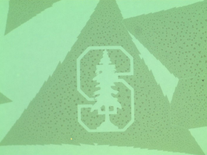
The researchers etched a nanoscale image of the Stanford tree onto an ultrathin chip, using the same technique that could one day create electronic circuits. (Image credit: Pop Lab)
But as researchers think about electronics for the next 50 years, they’ve begun to look beyond silicon to new types of materials that occur in single layers only three atoms thick – far thinner than modern silicon chips – yet are able to control electricity more efficiently to create those digital ones and zeroes.
Now a team led by Stanford electrical engineering Associate Professor Eric Pop has demonstrated how it might be possible to mass-produce such atomically thin materials and electronics. Why would this be useful? Because such thin materials would be transparent and flexible as well, in ways that would enable electronic devices that wouldn’t be possible to make with silicon.
“What if your window was also a television, or you could have a heads-up display on the windshield of your car?” asked Kirby Smithe, a graduate student on Pop’s team, suggesting electronic applications that the new materials might make possible.
Smithe, Pop and co-authors Chris English and Saurabh Suryavanshi, both graduate students in Pop’s lab, have described their work in the journal 2D Materials, which is dedicated to research into atomically thin, two-dimensional devices.
Theory into reality
The team’s goal was to develop a manufacturing process to turn single-layer chips into practical realities. The first atomically thin material was measured in 2004 when scientists observed that graphene – a material related to the “lead” in pencils – could be isolated in layers the thickness of a single carbon atom. The scientists who made this finding shared the 2010 Nobel Prize in Physics.
But the process used to make that discovery – the scientists lifted layers of graphene off a rock using sticky tape – was of no use in turning ultrathin crystals into next-generation electronics.
In the wake of the graphene discovery, engineers embarked on a quest to find similar materials and, more importantly, practical ways to fashion atomically thin switches into circuits.
It is on the issue of manufacturability where the Stanford team members made a big advance. They started with a single layer of material called molybdenum disulfide. The name describes its sandwich-like structure: a sheet of molybdenum atoms between two layers of sulfur. Previous research had shown that molybdenum disulfide made a good switch, controlling electricity to create digital ones and zeroes.
Scaling up
The question was whether the team could manufacture a molybdenum disulfide crystal big enough to form a chip. That requires building a crystal roughly the size of your thumbnail. This may not sound like a big deal until you consider the aspect ratio of the crystal required: a chip just three atoms thick but the size of your thumbnail is like a single sheet of paper big enough to cover the entire Stanford campus.
The Stanford team manufactured that sheet by depositing three layers of atoms into a crystalline structure 25 million times wider than it is thick. Smithe achieved this by making ingenious refinements to a manufacturing process called chemical vapor deposition. This approach essentially incinerates small amounts of sulfur and molybdenum until the atoms vaporize like soot. The atoms then deposit as an ultra-thin crystalline layer on a “handle” substrate, which can be glass or even silicon.
However, the researchers’ job was not done. They still had to pattern the material into electrical switches and to understand their operation. For this, they made use of a recent advance led by English, who discovered that extremely clean deposition conditions are essential to form good metallic contacts with the molybdenum disulfide layers. The wealth of new experimental data available now in the lab has also enabled Suryavanshi to craft accurate computer models of the new materials and to begin predicting their collective behavior as circuit components.
“We have a lot of work ahead to scale this process into circuits with larger scales and better performance,” Pop said. “But we now have all the building blocks.”
Etching the switches
During chip manufacturing, circuits must be etched into the material. To demonstrate how a large-scale, single-layer chip manufacturing process might perform this step in the future, the team used standard etching tools to cut the Stanford logo into their prototype. And then, to have a bit of fun with a project they completed during a national election campaign, they carved nanoscale portraits of the two major party candidates into their atomically thin canvas.
Pop said the Stanford team was inspired to do this by researchers who did something similar during the 2008 election cycle, when they created “nanobama” – minuscule images of then President-elect Barack Obama using carbon nanotubes. Nanotubes are another potential next-generation chip technology; the researchers on that project used nanobama as a way to call attention to the ability of technologists to manufacture objects that are almost unimaginably tiny.
“Many people are interested in electronics because the technology is useful,” Pop said. “But we hope nanotrump and nanoclinton can broaden the interest in research. Perhaps seeing portraits etched into a three-atom-thick canvas will inspire future researchers in ways we can’t even imagine yet.”
Eric Pop is also a member of the Precourt Institute for Energy.
This work was supported in part by the Air Force Office of Scientific Research, the National Science Foundation, the Semiconductor Research Corporation and the Stanford SystemX Alliance.
Media Contacts
Tom Abate, Stanford Engineering: (650) 736-2245, tabate@stanford.edu