Go to the web site to view the video.
A solar cell is basically a semiconductor, which converts sunlight into electricity, sandwiched between metal contacts that carry the electrical current.
But this widely used design has a flaw: The critical but shiny metal on top of the cell reflects sunlight away from the semiconductor where electricity is produced, reducing the cell’s efficiency.
Now Stanford scientists have discovered how to hide the reflective upper contact and funnel light directly to the semiconductor below. Their findings, published in the journal ACS Nano, could lead to a new paradigm in the design and fabrication of solar cells. (See video here.)
“Using nanotechnology, we have developed a novel way to make the upper metal contact nearly invisible to incoming light,” said study lead author Vijay Narasimhan, who conducted the work as a graduate student at Stanford. “Our new technique could significantly improve the efficiency and thereby lower the cost of solar cells.”
Mirror-like metal

Researchers in Associate Professor Yi Cui’s lab – including, from left, graduate students Vijay Narasimhan, Ruby Lai and Thomas Hymel – have discovered how to make the metal contacts on the surface of solar cells nearly invisible to incoming light. The new technique could significantly improve solar-cell efficiency. (Image credit: Mark Shwartz/Precourt Institute for Energy)
In most solar cells, the upper contact consists of a metal wire grid that carries electricity to or from the device. But these wires also act like a mirror and prevent sunlight from reaching the semiconductor, which is usually made of silicon.
“The more metal you have on the surface, the more light you block,” said study co-author Yi Cui, an associate professor of materials science and engineering. “That light is then lost and cannot be converted to electricity.”
Metal contacts, therefore, face a seemingly irreconcilable tradeoff between electrical conductivity and optical transparency, Narasimhan said. “But the nanostructure we created eliminates that tradeoff.”
For the study, the Stanford team placed a 16-nanometer-thick film of gold conducting metal on a flat sheet of silicon. The gold film was riddled with an array of nanosized square holes, but to the eye, the surface looked like a shiny, gold mirror.
Optical analysis revealed that the perforated gold film covered 65 percent of the silicon surface and reflected, on average, 50 percent of the incoming light. The scientists reasoned that if they could somehow hide the reflective gold film, more light would reach the silicon semiconductor below.
Silicon nanopillars
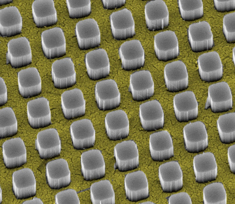
The solution: Create nanosized pillars of silicon that “tower” above the gold film and redirect the sunlight before it hits the metallic surface.
Creating silicon nanopillars turned out to be a one-step chemical process.
“We immersed the silicon and the perforated gold film together in a solution of hydrofluoric acid and hydrogen peroxide,” said graduate student and study co-author Thomas Hymel. “The gold film immediately began sinking into the silicon substrate, and silicon nanopillars began popping up through the holes in the film.”
Within seconds, the silicon pillars grew to a height of 330 nanometers, transforming the shiny gold surface to a dark red. This dramatic color change was a clear indication that the metal was no longer reflecting light.
“As soon as the silicon nanopillars began to emerge, they started funneling light around the metal grid and into the silicon substrate underneath,” Narasimhan explained.
He compared the nanopillar array to a colander in a kitchen sink.
“When you turn on the faucet, not all of the water makes it through the holes in the colander,” he said. “But if you were to put a tiny funnel on top of each hole, most of the water would flow straight through with no problem. That’s essentially what our structure does: The nanopillars act as funnels that capture light and guide it into the silicon substrate through the holes in the metal grid.”
The research team then optimized the design through a series of simulations and experiments.

Silicon nanopillars funnel light through a gold metal contact to a sheet of silicon underneath. (Image credit: Vijay Narasimhan)
“Solar cells are typically shaded by metal wires that cover 5 to 10 percent of the top surface,” Narasimhan said. “In our best design, nearly two-thirds of the surface can be covered with metal, yet the reflection loss is only 3 percent. Having that much metal could increase conductivity and make the cell far more efficient at converting light to electricity.”
For example, this technology could boost the efficiency of a conventional solar cell from 20 percent to 22 percent, a significant increase, he said.
The research team plans to test the design on a working solar cell and assess its performance in real-world conditions.
Covert contacts
Besides gold, the nanopillar architecture will also work with contacts made of silver, platinum, nickel and other metals, said graduate student and co-author Ruby Lai.
“We call them ‘covert contacts,’ because the metal hides in the shadows of the silicon nanopillars,” she said. “It doesn’t matter what type of metal you put in there. It will be nearly invisible to incoming light.”
In addition to silicon, this new technology can be used with other semiconducting materials for a variety of applications, including photosensors, light-emitting diodes and displays and transparent batteries, as well as solar cells.
“With most optoelectronic devices, you typically build the semiconductor and the metal contacts separately,” said Cui, co-director of the Department of Energy’s Bay Area Photovoltaic Consortium (BAPVC). “Our results suggest a new paradigm where these components are designed and fabricated together to create a high-performance interface.”
On Dec. 1, Cui and Narasimhan will discuss the new nanopillar technology at the fall meeting of the Materials Research Society in Boston.
The study was supported by the BAPVC and the Global Climate and Energy Project at Stanford.
Media Contacts
Mark Shwartz, Precourt Institute for Energy: (650) 723-9296, mshwartz@stanford.edu
Yi Cui, Materials Science and Engineering: (650) 723-4613, yicui@stanford.edu