|
November 16, 2011
Sorting out the nanotubes, for better electronics
A new technique developed by Stanford researchers advances commercial potential of semiconducting carbon nanotubes for printable circuits, bendable display screens, stretchable electronics and solar technology. By Sarah Jane Keller
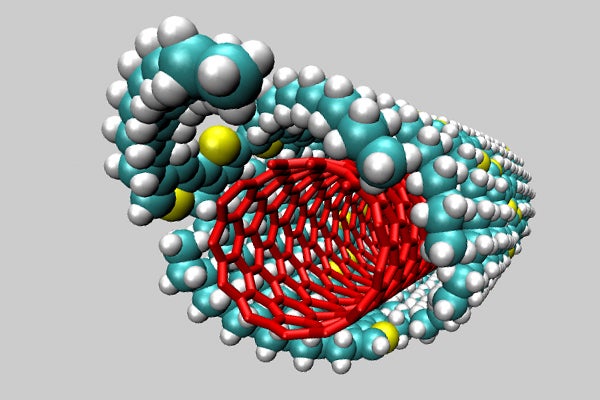
A computer-generated cross section of the polymer-coated carbon nanotube. The polymer shell (blue) wraps around a semiconducting single-walled carbon nanotube (red). (Photo: Francois Gygi and Giulia Galli / UC-Davis) Carbon nanotubes could make many electronic devices cheaper and more efficient. But when nanotubes are manufactured, tubes that work for solar cells are mixed with tubes that work for batteries. The final product is a nanotube powder that is not ideal for any single commercial application.
Zhenan Bao, Stanford associate professor of chemical engineering, and her colleagues at University of California-Davis and the Samsung Advanced Institute of Technology have discovered a technique to selectively sort semiconducting single-walled carbon nanotubes from the mixture. The results appear online in Nature Communications.
The semiconducting nanotubes could be used in flexible transistors for other technologies that Bao's group develops, including circuits printed on plastic, bendable display screens and stretchable electronics. The nanotubes could also close gaps in solar cell technology.
"Sorting has been a major bottleneck for carbon nanotubes to be viable for practical electronics applications," Bao said. "This work solves the problem of separating the conducting from the semiconducting nanotubes."
Conducting tubes are used in wires and electrodes but semiconducting tubes are the active material for transistors or solar cells. Mixtures of conducting and semiconducting tubes do not carry enough current for wires or battery electrodes. And when the mixture is used for semiconducting, as in a transistor, the excess current from the conducting nanotubes will short the device.
Bao's group uses a polymer that selectively sorts the mixture by wrapping around semiconducting nanotubes, and not conducting nanotubes. Mixing the polymer with commercially available carbon nanotubes in a solvent separates semiconducting tubes from conducting tubes.
In her past work with the polymer, Bao was the first to find that it has good semiconducting properties in transistors. It is now the most widely studied polymer for plastic circuits and plastic transistors and also for plastic solar cells. Bao's group is the first to combine it with semiconducting carbon nanotubes.
This is not the first time a polymer has been used to sort conducting and semiconducting nanotubes. However, past polymers have insulated the nanotubes and required extensive removal treatments to restore the conductivity of the nanotubes.
The polymer in Bao's process does not need to be removed. The final product is a semiconducting nanotube and polymer ink that can be used to make printable electronics.
"Our simple process allows us to build useful devices very easily," she said.
The group tested nearly 200 individual nanotubes to confirm that the polymer only wraps around semiconducting tubes and not conducting tubes. To explain how the polymer wraps around the carbon nanotube, UC-Davis collaborators Giulia Galli and Francois Gygi modeled the geometry of a semiconducting carbon nanotube and its polymer shell.
According to Galli, the model provides "a theoretical explanation of how this polymer actually interacts with the nanotube." The polymer has a long, rigid backbone, with regular arm-like molecular chains along each side. The side chains fit together like fingers, making a ribbon of polymer that wraps around the semiconducting nanotubes.
Bao's work with nanotubes is part of her long-term collaboration with the Samsung Advanced Institute of Technology. "I'm especially happy that this polymer can now be used to sort nanotubes," Bao said. "It merges two very important materials together and makes a hybrid material that could be very useful for printed and flexible electronics."
Jeffrey B.-H. Tok, senior research engineer; Andrew Spakowitz, assistant professor of chemical engineering; and H.S.Philip Wong, professor of electrical engineering, contributed to the research. Chemical engineering graduate student Hang Woo Lee, materials science and engineering graduate students Steve Park and Huiliang Wang also contributed, as well as Satoshi Morishita of chemical engineering, Luckshitha S. Liyanage of electrical engineering and Nishant Patil of electrical engineering.
The Samsung Advanced Institute of Technology and the National Science Foundation provided funding for the research.
Sarah Jane Keller is a science-writing intern at the Stanford News Service.
-30-
|


