
A new material could enable more efficient magnet-based computer memory
Engineers have found a metallic compound that could bring more efficient forms of computer memory closer to commercialization, reducing computing’s carbon footprint, enabling faster processing, and allowing AI training to happen on individual devices instead of remote servers.
Over the last decade, with the introduction of increasingly complex artificial intelligence (AI) technologies, the demand for computing power has risen exponentially. New, energy-efficient hardware designs could help meet this demand while reducing computing’s energy use, supporting faster processing, and allowing AI training to take place within the device itself.
The spin orbit torque magnetoresistive random access memory (SOT-MRAM) has the potential to store data more quickly and efficiently than current methods, which store data using electric charge and require a continuous power input to maintain that data. (Image credit: Shutterstock/raigvi)
“In my opinion, we have already transitioned from the internet era to the AI era,” says Shan Wang, the Leland T. Edwards Professor in the School of Engineering at Stanford University. “We want to enable AI on edge – training locally on your home computer, phone, or smartwatch – for things like heart attack detection or speech recognition. To do that, you need a very fast, non-volatile memory.”
Wang and his colleagues recently found a material that could bring a new type of memory closer to commercialization. In a new paper published in Nature Materials, the researchers demonstrated that a thin layer of a metallic compound called manganese palladium three had the necessary properties to facilitate a form of working memory that stores data in electron spin directions. This method of memory storage, known as spin orbit torque magnetoresistive random access memory or SOT-MRAM, has the potential to store data more quickly and efficiently than current methods, which store data using electric charge and require a continuous power input to maintain that data.
“We’ve provided a basic building block for future energy-efficient storage elements,” Wang says. “It’s very foundational, but it’s a breakthrough.”
Harnessing electron spin
SOT-MRAM relies on an intrinsic property of electrons called spin. To understand spin, picture an electron as a rotating basketball balanced on the end of a professional athlete’s finger. Because electrons are charged particles, the rotation turns the electron into a tiny magnet, polarized along its axis (in this case, a line that extends from the finger balancing the ball). If the electron switches spin directions, the north-south poles of the magnet switch. Researchers can use the up or down direction of that magnetism – known as the magnetic dipole moment – to represent the ones and zeroes that make up bits and bytes of computer data.
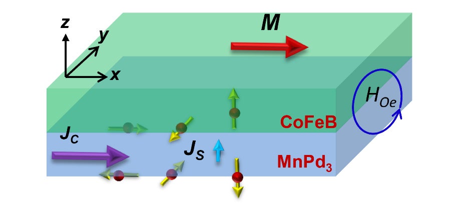
Unconventional z-spin polarization in MnPd3 material. (Image credit: The Wang Group)
In SOT-MRAM, a current flowing through one material (the SOT layer) generates specific spin directions. The movement of those electrons, coupled with their spin directions, creates a torque that can switch the spin directions and associated magnetic dipole moments of electrons in an adjacent magnetic material. With the right materials, storing magnetic data is as simple as switching the direction of an electrical current in the SOT layer.
But finding the right SOT materials isn’t easy. Because of the way the hardware is designed, data can be stored more densely when electron spin directions are oriented up or down in the z-direction. (If you imagine a sandwich on a plate, the x- and y-directions follow the edges of the bread and the z-direction is the toothpick shoved through the middle.) Unfortunately, most materials polarize electron spins in the y-direction if the current flows in the x-direction.
“Conventional materials only generate spin in the y-direction – that means we would need an external magnetic field to make switching happen in the z-direction, which takes more energy and space,” says Fen Xue, a postdoctoral researcher in Wang’s lab. “For the purpose of lowering the energy and having a higher density of memory, we want to be able to realize this switching without an external magnetic field.”
The researchers found that manganese palladium three has the properties they need. The material is able to generate spins in any orientation because its internal structure lacks the kind of crystal symmetry that would force all of the electrons into a particular orientation. Using manganese palladium three, the researchers were able to demonstrate magnetization switching in both the y- and z-directions without needing an external magnetic field. Although not demonstrated in the manuscript, x-direction magnetization can also be switched in the absence of external magnetic field.
“We have the same input current as other conventional materials, but we have three different directions of spins now,” says Mahendra DC, who conducted the work as a postdoctoral researcher at Stanford and is first author on the paper. “Depending on the application, we can control the magnetization in whatever direction we want.”
DC and Wang credit the multidisciplinary and multi-institutional collaboration that enabled these advances. “Evgeny Tsymbal’s lab at the University of Nebraska led the calculations to predict the unexpected spin directions and movement and Julie Borchers’s lab at the National Institute of Standards and Technology led the measurements and modeling efforts to reveal the intricate microstructures within manganese palladium three,” says Wang. “It truly takes a village.”
Manufacturing possibilities
In addition to its symmetry-breaking structure, manganese palladium three has several other properties that make it an excellent candidate for SOT-MRAM applications. It can, for example, survive and maintain its properties through the post-annealing process that electronics need to go through.
“Post-annealing requires electronics to be at 400 degrees Celsius for 30 minutes,” DC says. “That’s one of the challenges for new materials in these devices, and manganese palladium three can handle that.”
Also, the layer of manganese palladium three is created using a process called magnetron sputtering, which is a technique that is already used in other aspects of memory-storage hardware.
“There’s no new tools or new techniques needed for this kind of material,” Xue says. “We don’t need a textured substrate or special conditions to deposit it.”
The result is a material that not only has novel properties that could help meet our growing computing requirements, but can fit smoothly into current manufacturing techniques. The researchers are already working on prototypes of SOT-MRAM using manganese palladium three that will integrate into real devices.
“We are hitting a wall with the current technology,” DC says. “So we have to figure out what other options we have.”
Wang is a professor of Materials Science and Engineering, and jointly of Electrical Engineering, a member of Geballe Laboratory of Advanced Materials, Stanford Bio-X, and the Wu Tsai Neurosciences Institute; and an affiliate of the Precourt Institute for Energy and the Stanford Woods Institute for the Environment.
Additional Stanford co-authors of this research include senior research scientist Arturas Vailionis, adjunct professor Wilman Tsai, research consultant Chong Bi, research associate Xiang Li, and graduate student Yong Deng. Other coauthors are from University of Nebraska, Taiwan Semiconductor Manufacturing Company, Kaunas University of Technology, National Institute of Standards and Technology, University of Arizona, Colorado School of Mines, National Yang Ming Chiao Tung University, Seikei University.
This work was funded by Semiconductor Research Corporation (SRC); Defense Advanced Research Projects Agency; the National Science Foundation; the National Research Council; Center for Semiconductor Technology Research; the National Science and Technology Council, Taiwan; JSPS KAKENHI; Heiwa Nakajima Foundation; PMAC for Science Research Promotion Fund; and JST-FOREST. Part of this work was performed at the Stanford Nano Shared Facilities (SNSF)/Stanford Nanofabrication Facility (SNF).
To read all stories about Stanford science, subscribe to the biweekly Stanford Science Digest.