|
April 3, 2012
Straintronics: Stanford engineers create piezoelectric graphene
By depositing atoms on one side of a grid of the "miracle material" graphene, researchers at Stanford have engineered piezoelectricity into a nanoscale material for the first time. Twist it and it generates electricity. The implications could yield a dramatic degree of control in nanotechnology. By Andrew Myers
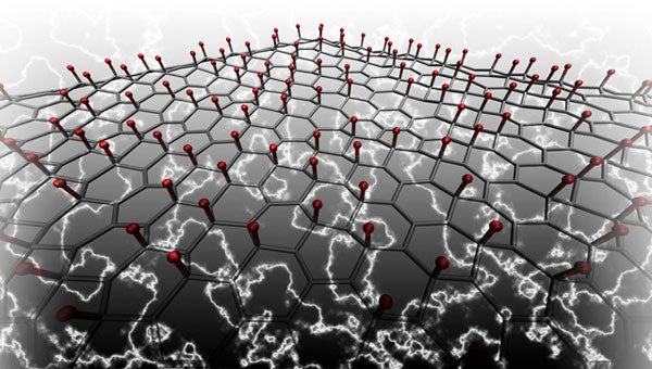
This illustration shows lithium atoms (red) adhered to a graphene lattice that will produce electricity when bent, squeezed or twisted. Conversely, the graphene will deform when an electric field is applied, opening new possibilities in nanotechnology. (Illustration: Mitchell Ong / Stanford School of Engineering) To the long list of exceptional physical properties of graphene, Stanford engineers have added yet another: piezoelectricity, the property of some materials to produce an electric charge when bent, squeezed or twisted. The results were described recently in a paper published in the journal ACSNano.
In what became known as the "Scotch tape technique," researchers first extracted graphene with a piece of adhesive in 2004. Graphene is a single layer of carbon atoms arranged in a honeycomb, hexagonal pattern. Under a microscope, it looks like chicken wire. In 2010, the researchers who first isolated it shared the Nobel Prize.
Graphene is a wonder material. It is a hundred times better at conducting electricity than silicon. It is stronger than diamond. And, at just one atom thick, it is so thin as to be essentially a two-dimensional material. Such promising physics have made graphene the most studied substance of the last decade, particularly in nanotechnology.
Yet, while graphene is many things, it is not piezoelectric.
Perhaps most valuably, piezoelectricity is reversible. When an electric field is applied, piezoelectric materials change shape, yielding a remarkable level of engineering control.
Piezoelectrics have found application in countless devices from watches, radios and ultrasound to the push-button starters on propane grills, but these uses all require relatively large, three-dimensional quantities of piezoelectric materials.
The Stanford team's engineered graphene has, for the first time, extended such fine physical control to the nanoscale.
Straintronics
"The physical deformations we can create are directly proportional to the electrical field applied and this represents a fundamentally new way to control electronics at the nanoscale," said Evan Reed, head of the Materials Computation and Theory Group at Stanford and senior author of the study. "This phenomenon brings new dimension to the concept of 'straintronics' for the way the electrical field strains — or deforms — the lattice of carbon, causing it to change shape in predictable ways."
"Piezoelectric graphene could provide an unparalleled degree of electrical, optical or mechanical control for applications ranging from touchscreens to nanoscale transistors," said Mitchell Ong, a post-doctoral scholar in Reed's lab and first author of the paper.
Using a sophisticated modeling application running on high-performance supercomputers, the engineers simulated the deposition of atoms on one side of a graphene lattice – a process known as doping – and measured the piezoelectric effect.
They modeled graphene doped with lithium, hydrogen, potassium and fluorine, as well as combinations of hydrogen and fluorine and lithium and fluorine, on either side of the lattice. Doping just one side of the graphene, or doping both sides with different atoms, is key to the process as it breaks graphene's perfect physical symmetry, which otherwise cancels the piezoelectric effect.
The results surprised both engineers.
"We thought the piezoelectric effect would be present, but relatively small. Yet, we were able to achieve piezoelectric levels comparable to traditional three-dimensional materials," said Reed. "It was pretty significant."
Designer piezoelectricity
"We were further able to fine tune the effect by pattern-doping the graphene – selectively placing atoms in specific sections and not others," said Ong. "We call it designer piezoelectricity because it allows us to strategically control where, when and how much the graphene is deformed by an applied electrical field with promising implications for engineering."
While the results in creating piezoelectric graphene are encouraging, the researchers believe that their technique might further be used to engineer piezoelectricity in nanotubes and other nanomaterials with applications ranging from electronics, photonics and energy harvesting to chemical sensing and high-frequency acoustics.
"We're already looking now at new piezoelectric devices based on other 2D and low-dimensional materials hoping they might open new and dramatic possibilities in nanotechnology," said Reed.
The Army High Performance Computing Research Center at Stanford University and the National Energy Research Scientific Computing Center (NERSC) at the Lawrence Berkeley National Laboratory supported this research.
Andrew Myers is the associate director of communications for the Stanford School of Engineeri
-30-
|


