|
February 13, 2012
Stanford engineers weld nanowires with light
At the nano level, researchers at Stanford have discovered a new way to weld together meshes of tiny wires. Their work could lead to innovative electronics and solar applications. To succeed, they called upon plasmonics. By Andrew Myers
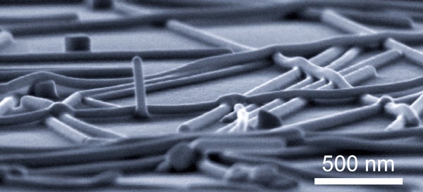
A bright burst of light has welded these nanowires together. (Photo: Courtesy of Stanford School of Engineering) One area of intensive research at the nanoscale is the creation of electrically conductive meshes made of metal nanowires. Promising exceptional electrical throughput, low cost and easy processing, engineers foresee a day when such meshes are common in new generations of touchscreens, video displays, light-emitting diodes and thin-film solar cells.
Standing in the way, however, is a major engineering hurdle: In processing, these delicate meshes must be heated or pressed to unite the crisscross pattern of nanowires that form the mesh, and are thereby damaged.
In a paper just published in the journal Nature Materials, a team of engineers at Stanford has demonstrated a promising new nanowire welding technique that harnesses plasmonics to fuse the wires with a simple blast of light.
Self-limiting
At the heart of the technique is the physics of plasmonics, the interaction of light and metal in which the light flows across the surface of the metal in waves, like water on the beach.
"When two nanowires lay criss-crossed, we know that light will generate plasmon waves at the place where the two nanowires meet, creating a hot spot. The beauty is that the hot spots exist only when the nanowires touch, not after they have fused. The welding stops itself. It's self-limiting," explained Mark Brongersma, associate professor of materials science and engineering at Stanford and an expert in plasmonics. Brongersma is one of the study's senior authors.
"The rest of the wires and, just as importantly, the underlying material are unaffected," noted Michael McGehee, also an associate professor of materials science and engineering and a senior author of the paper. "This ability to heat with precision greatly increases the control, speed and energy efficiency of nanoscale welding."
In before-and-after electron-microscope images, individual nanowires are visually distinct prior to illumination. They lie atop one another, like fallen trees in the forest. When illuminated, the top nanowire acts like an antenna of sorts, directing the plasmon waves of light into the bottom wire and creating heat that welds the wires together. Post-illumination images show X-like nanowires lying flat against the substrate with fused joints.
Transparency
In addition to making it easier to produce stronger and better-performing nanowire meshes, the researchers say that the new technique could open the possibility of mesh electrodes bound to flexible or transparent plastics and polymers.
To demonstrate the possibilities, they applied their mesh on Saran wrap. They sprayed a solution containing silver nanowires in suspension on the plastic and dried it. After illumination, what was left was an ultrathin layer of welded nanowires.
"Then we balled it up like a piece of paper. When we unfurled the wrap, it maintained its electrical properties," said co-author Yi Cui, associate professor of materials science and engineering. "And when you hold it up, it's virtually transparent."
This could lead to inexpensive window coatings that generate solar power while reducing glare for those inside, the researchers said.
"In previous welding techniques that used a hotplate, this would never have been possible," said the paper's lead author, Erik C. Garnett, a postdoctoral scholar in materials science who works with Brongersma, McGehee and Cui. "The Saran wrap would have melted far sooner than the silver, destroying the device instantly."
"There are many possible applications that would not even be possible in older annealing techniques," said Brongersma. "This opens some interesting, simple and large-area processing schemes for electronic devices – solar, LEDs and touchscreen displays, especially."
The research was supported by the Center for Advanced Molecular Photovoltaics (CAMP) at Stanford University, funded by King Abdullah University of Science and Technology (KAUST).
Andrew Myers is associate director of communications at the School of Engineering.
-30-
|


